SPI NOR - NOR 存储器件
本文将讲述 V821 搭配 SPI NOR 作为存储设备使用的相关配置,新物料支持等说明。V821 SPIF 控制器功能如下:
SPI Flash 控制器(SPiF)是一个同步的串行通信接口,允许以更少的软件中断进行快速的数据通信。与 SPI 不同,SPiF 通常设计用于更高速的 Flash 设备,并且仅在 Master 模式下工作。
- 支持多种 SPI 模式
- 标准 SPI
- 双输出/双输入 SPI 和双 I/O SPI
- 四输出/四输入 SPI、Quad I/O 和 QPI
- 可编程串行数据帧长度
- 1 位到 32 位
- 支持单速率传输(STR)模式和双速率传输(DTR)模式
- 高速时钟频率
- 150 MHz(STR 模式)
- 100 MHz(DTR 模式)
- 软件写保护
- 通过软件实现对全部或部分存储区的写保护
- 顶部/底部块保护
- 可编程事务间延迟
- 支持模式 0 模式 1 模式 2 和模式 3
- 支持控制信号配置
- 一个片选信号支持多个外设
- 芯片选择(SPIF_CS)和 SPI 时钟(SPIF_CLK)的极性和相位可配置
SPI NOR 新物料适配
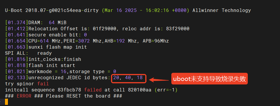
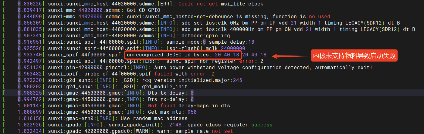
未适配 SPI NOR 物料的报错
U-Boot 未支持物料导致烧录失败:
Kernel 未支持物料导致启动失败:
了解新物料的特性
在拿到一款 SPI NOR 物料时,需要仔细阅读其手册。下图是 PY25Q256HB 物料的介绍页,可以看出支持 SPI,Dual SPI,QPI,DTR 模式,支持 4K 擦写。

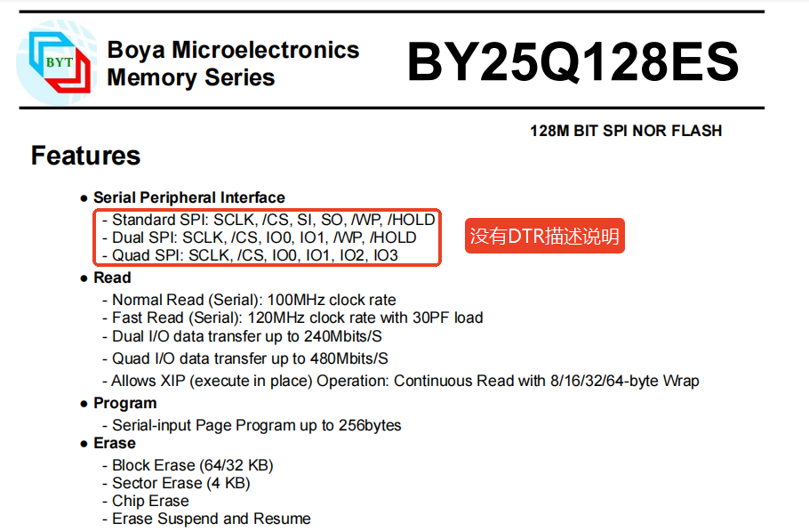
换一个物料 BY25Q128ES,手册中没有提到 DTR,这款物料不支持 DTR 模式。
在文档后面电器参数章节,可以找到其运行的最高主频,在之后配置中需要小于这里的最高频率,切勿超频运行。

部分 NOR 手册中还会标明其不同模式下支持的速率,可以作为参考
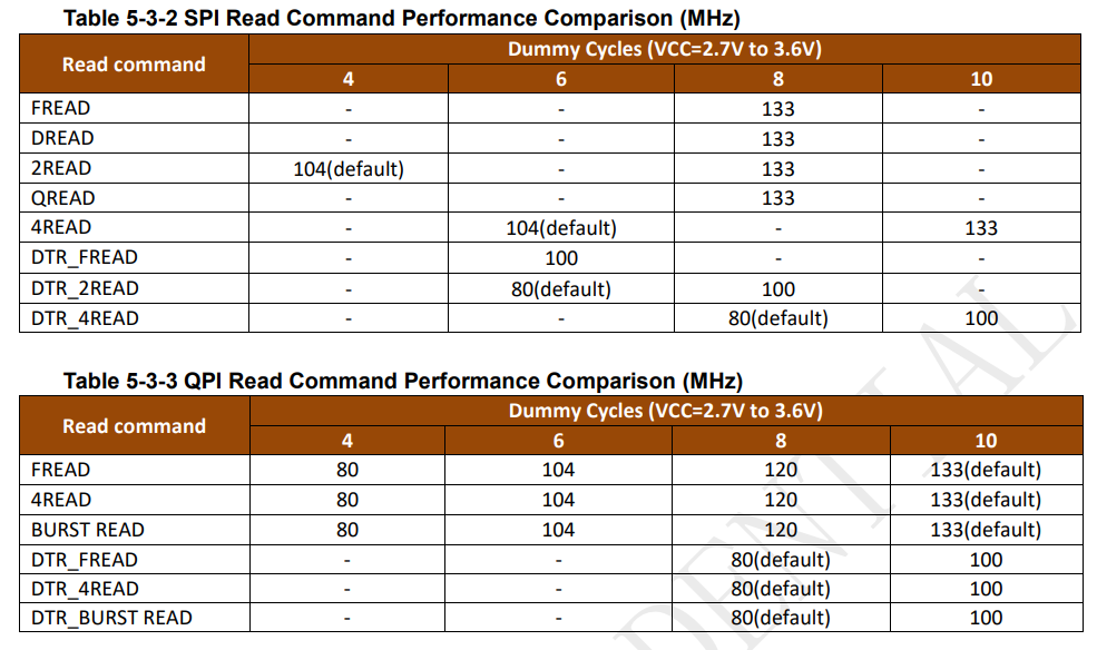
- 在 DTR 模式下默认 80M,读指令10可以支持100M
一般在文档末尾可以找到 SPI NOR 物料的器件 ID,适配新物料时需要重点关注。

- ID 是
0x852019
还可以找到 NOR 物料的内存布局
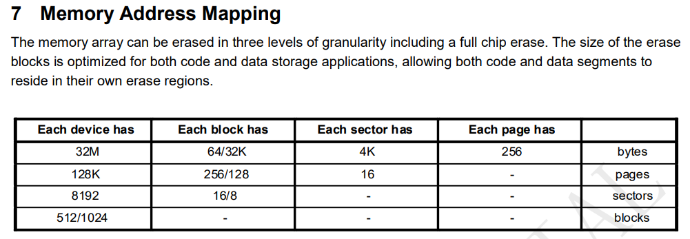
- 每个存储设备有 32MByte 空间
- 每个块(扇区)有 64K(或者32K)
- 总共有512(或1024)个块(扇区)
一般使用 64K 模式,则 NOR 物料为 64K * 512 = 32MByte
适配 U-Boot 驱动
添加新物料,U-Boot 需要修改文件 brandy/brandy-2.0/u-boot-2018/drivers/mtd/spi/spi-nor-ids.c,U-Boot 使用一个列表存放支持的物料。我们只需要把新增的物料加入列表即可。
可以先找一下类型生产厂家的型号,例如这里找 PUYA 的型号,加上新物料 py25q256hb
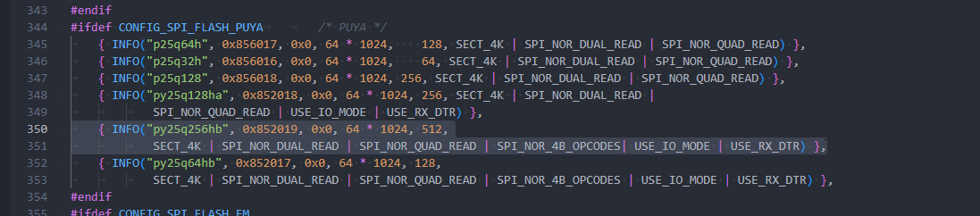
这里通过 INFO 宏定义了一个设备的信息,包括设备名称、ID、扇区大小、扇区数量、页面大小和一些设备特性。还有一个 INFO6 宏,如果芯片的 EXT_ID 较多可以使用这个宏。
1. 宏定义部分
#define INFO(_name, _jedec_id, _ext_id, _sector_size, _n_sectors, _flags) \
        INFO_NAME(_name) \
        .id = { \
            ((_jedec_id) >> 16) & 0xff, \
            ((_jedec_id) >> 8) & 0xff, \
            (_jedec_id) & 0xff, \
            ((_ext_id) >> 8) & 0xff, \
            (_ext_id) & 0xff, \
        }, \
        .id_len = (!(_jedec_id) ? 0 : (3 + ((_ext_id) ? 2 : 0))), \
        .sector_size = (_sector_size), \
        .n_sectors = (_n_sectors), \
        .page_size = 256, \
        .flags = (_flags),
- INFO宏:这个宏用于定义设备的一些基本信息。它接受六个参数:
_name:设备名称。_jedec_id:设备的JEDEC ID。_ext_id:扩展ID。_sector_size:扇区大小。_n_sectors:扇区数量。_flags:标志,通常是 SPI NOR 的一些附加的配置或特性。
2. 宏中的内容
- INFO_NAME(_name):宏调用
INFO_NAME,传递设备的名称_name。 - .id:这部分将
_jedec_id和_ext_id以特定的方式拆分为字节数组。具体拆分方法:- 将
_jedec_id右移16位、8位、0位,分别取出低8位,组成前三个字节。 - 将
_ext_id右移8位、0位,分别取出低8位,组成后两个字节。 结果是将jedec_id和ext_id组合成一个5字节的 ID,通常是一个设备标识符。
- 将
- .id_len:根据
jedec_id和ext_id是否为0来计算 ID 的长度。具体来说:- 如果
jedec_id为0,表示没有有效的 ID,ID 长度为0。 - 否则,ID 长度是3(固定的前3个字节),如果
ext_id非零,则再加2个字节。
- 如果
- .sector_size:设置扇区的大小为
_sector_size。 - .n_sectors:设置设备的扇区数量为
_n_sectors。 - .page_size:设置页面大小为256字节,这个值是固定的。
- .flags:设置设备的一些标志(如双读、四读、4字节操作码、使用IO模式等)。
3. 使用这个宏的实例
{ INFO("py25q256hb", 0x852019, 0x0, 64 * 1024, 512, SECT_4K | SPI_NOR_DUAL_READ | SPI_NOR_QUAD_READ | SPI_NOR_4B_OPCODES | USE_IO_MODE | USE_RX_DTR) }
- "py25q256hb":设备的名称。
- 0x852019:设备的JEDEC ID。
- 0x0:扩展ID,这里是0,表示没有扩展ID。
- 64 * 1024:扇区大小为64KB。
- 512:扇区数量为512个。
- SECT_4K | SPI_NOR_DUAL_READ | SPI_NOR_QUAD_READ | SPI_NOR_4B_OPCODES | USE_IO_MODE | USE_RX_DTR:这些是设备的特性标志。每个标志位的作用如下:
SECT_4K:表示扇区大小是4KB。SPI_NOR_DUAL_READ:支持SPI NOR的双读模式。SPI_NOR_QUAD_READ:支持SPI NOR的四读模式。SPI_NOR_4B_OPCODES:支持4字节操作码,大于128Mib(16MByte)的设备需要配置。USE_IO_MODE:使用IO模式。USE_RX_DTR:使用接收数据传输模式。
完整的标志位及其含义如下表所示:
| 标志位 | 位掩码 | 描述 |
|---|---|---|
| SECT_4K | BIT(0) | 支持4KB的扇区。 |
| SPI_NOR_NO_ERASE | BIT(1) | 不需要擦除命令。 |
| SST_WRITE | BIT(2) | 使用SST字节编程模式。 |
| SPI_NOR_NO_FR | BIT(3) | 不支持快速读取模式。 |
| SECT_4K_PMC | BIT(4) | 支持4KB扇区PMC操作。 |
| SPI_NOR_DUAL_READ | BIT(5) | 支持双读模式(Dual Read)。 |
| SPI_NOR_QUAD_READ | BIT(6) | 支持四读模式(Quad Read)。 |
| USE_FSR | BIT(7) | 使用标志状态寄存器(Flag Status Register)。 |
| SPI_NOR_HAS_LOCK | BIT(8) | 支持通过状态寄存器(SR)进行锁定/解锁操作。 |
| SPI_NOR_HAS_TB | BIT(9) | 状态寄存器(SR)支持顶部/底部保护(Top/Bottom Protect)。必须与 SPI_NOR_HAS_LOCK 一起使用。 |
| SPI_S3AN | BIT(10) | 支持Xilinx Spartan 3AN系列的系统闪存。该闪存的制造商ID与Atmel闪存相同,因此无法通过制造商ID进行区分。 |
| SPI_NOR_4B_OPCODES | BIT(11) | 使用专用的4字节地址操作码,支持128Mib以上的内存大小。 |
| NO_CHIP_ERASE | BIT(12) | 不支持芯片擦除。 |
| SPI_NOR_SKIP_SFDP | BIT(13) | 跳过解析SFDP表格。 |
| USE_CLSR | BIT(14) | 使用CLSR命令(Clear Status Register)。 |
| SPI_NOR_INDIVIDUAL_LOCK | BIT(16) | 支持单独的块/扇区锁定模式。 |
| SPI_NOR_HAS_LOCK_HANDLE | BIT(17) | 锁定操作支持有锁定句柄。 |
| SPI_NOR_OCTAL_READ | BIT(18) | 支持八通道读取模式(Octal Read)。 |
| USE_IO_MODE | BIT(19) | 支持地址和数据线宽度可变的IO模式。 |
| USE_RX_DTR | BIT(20) | 支持接收数据传输模式(RX DTR)。 |
| USE_TX_DTR | BIT(21) | 支持发送数据传输模式(TX DTR)。 |
| USE_DQS | BIT(22) | 支持DQS模式。 |
| OCTAL_SPINOR | BIT(23) | 支持八通道SPI NOR模式。 |
| SPI_NOR_STACK_DIE | BIT(24) | 支持使用多芯片堆叠(multi-die)操作。 |
适配 Kernel 驱动
添加新物料,Kernel 需要修改文件 bsp/drivers/mtd/spi-nor-5.4/spi-nor.c,Kernel 使用一个列表存放支持的物料。我们只需要把新增的物料加入列表即可。
可以先找一下类型生产厂家的型号,例如这里找 PUYA 的型号,加上新物料 py25q256hb

这里通过 INFO 宏定义了一个设备的信息,包括设备名称、ID、扇区大小、扇区数量、页面大小和一些设备特性。还有一个 INFO6 宏,如果芯片的 EXT_ID 较多可以使用这个宏。
#define INFO(_jedec_id, _ext_id, _sector_size, _n_sectors, _flags)	\
		.id = {							\
			((_jedec_id) >> 16) & 0xff,			\
			((_jedec_id) >> 8) & 0xff,			\
			(_jedec_id) & 0xff,				\
			((_ext_id) >> 8) & 0xff,			\
			(_ext_id) & 0xff,				\
			},						\
		.id_len = (!(_jedec_id) ? 0 : (3 + ((_ext_id) ? 2 : 0))),	\
		.sector_size = (_sector_size),				\
		.n_sectors = (_n_sectors),				\
		.page_size = 256,					\
		.flags = (_flags),
- INFO宏:这个宏用于定义设备的一些基本信息。它接受五个参数:
_jedec_id:设备的JEDEC ID。_ext_id:扩展ID。_sector_size:扇区大小。_n_sectors:扇区数量。_flags:标志,通常是 SPI NOR 的一些附加的配置或特性。
2. 宏中的内容
- .id:这部分将
_jedec_id和_ext_id以特定的方式拆分为字节数组。具体拆分方法:- 将
_jedec_id右移16位、8位、0位,分别取出低8位,组成前三个字节。 - 将
_ext_id右移8位、0位,分别取出低8位,组成后两个字节。 结果是将jedec_id和ext_id组合成一个5字节的 ID,通常是一个设备标识符。
- 将
- .id_len:根据
jedec_id和ext_id是否为0来计算 ID 的长度。具体来说:- 如果
jedec_id为0,表示没有有效的 ID,ID 长度为0。 - 否则,ID 长度是3(固定的前3个字节),如果
ext_id非零,则再加2个字节。
- 如果
- .sector_size:设置扇区的大小为
_sector_size。 - .n_sectors:设置设备的扇区数量为
_n_sectors。 - .page_size:设置页面大小为256字节,这个值是固定的。
- .flags:设置设备的一些标志(如双读、四读、4字节操作码、使用IO模式等)。
3. 使用这个宏的实例
INFO(0x852019, 0x0, 64 * 1024, 512, SECT_4K | SPI_NOR_DUAL_READ | SPI_NOR_QUAD_READ | SPI_NOR_4B_OPCODES | USE_IO_MODE | USE_RX_DTR)
- 0x852019:设备的JEDEC ID。
- 0x0:扩展ID,这里是0,表示没有扩展ID。
- 64 * 1024:扇区大小为64KB。
- 512:扇区数量为512个。
- SECT_4K | SPI_NOR_DUAL_READ | SPI_NOR_QUAD_READ | SPI_NOR_4B_OPCODES | USE_IO_MODE | USE_RX_DTR:这些是设备的特性标志。每个标志位的作用如下:
SECT_4K:表示扇区大小是4KB。SPI_NOR_DUAL_READ:支持SPI NOR的双读模式。SPI_NOR_QUAD_READ:支持SPI NOR的四读模式。SPI_NOR_4B_OPCODES:支持4字节操作码,大于128Mib(16MByte)的设备需要配置。USE_IO_MODE:使用IO模式。USE_RX_DTR:使用接收数据传输模式。
完整的标志位及其含义如下表所示:
| 标志位 | 位掩码 | 描述 |
|---|---|---|
| SECT_4K | BIT(0) | 支持4KB的扇区。 |
| SPI_NOR_NO_ERASE | BIT(1) | 不需要擦除命令。 |
| SST_WRITE | BIT(2) | 使用SST字节编程模式。 |
| SPI_NOR_NO_FR | BIT(3) | 不支持快速读取模式。 |
| SECT_4K_PMC | BIT(4) | 支持4KB扇区PMC操作。 |
| SPI_NOR_DUAL_READ | BIT(5) | 支持双读模式(Dual Read)。 |
| SPI_NOR_QUAD_READ | BIT(6) | 支持四读模式(Quad Read)。 |
| USE_FSR | BIT(7) | 使用标志状态寄存器(Flag Status Register)。 |
| SPI_NOR_HAS_LOCK | BIT(8) | 支持通过状态寄存器(SR)进行锁定/解锁操作。 |
| SPI_NOR_HAS_TB | BIT(9) | 状态寄存器(SR)支持顶部/底部保护(Top/Bottom Protect)。必须与 SPI_NOR_HAS_LOCK 一起使用。 |
| SPI_S3AN | BIT(10) | 支持Xilinx Spartan 3AN系列的系统闪存。该闪存的制造商ID与Atmel闪存相同,因此无法通过制造商ID进行区分。 |
| SPI_NOR_4B_OPCODES | BIT(11) | 使用专用的4字节地址操作码,支持128Mib以上的内存大小。 |
| NO_CHIP_ERASE | BIT(12) | 不支持芯片擦除。 |
| SPI_NOR_SKIP_SFDP | BIT(13) | 跳过解析SFDP表格。 |
| USE_CLSR | BIT(14) | 使用CLSR命令(Clear Status Register)。 |
| SPI_NOR_INDIVIDUAL_LOCK | BIT(16) | 支持单独的块/扇区锁定模式。 |
| SPI_NOR_HAS_LOCK_HANDLE | BIT(17) | 锁定操作支持有锁定句柄。 |
| SPI_NOR_OCTAL_READ | BIT(18) | 支持八通道读取模式(Octal Read)。 |
| USE_IO_MODE | BIT(19) | 支持地址和数据线宽度可变的IO模式。 |
| USE_RX_DTR | BIT(20) | 支持接收数据传输模式(RX DTR)。 |
| USE_TX_DTR | BIT(21) | 支持发送数据传输模式(TX DTR)。 |
| USE_DQS | BIT(22) | 支持DQS模式。 |
| OCTAL_SPINOR | BIT(23) | 支持八通道SPI NOR模式。 |
| SPI_NOR_STACK_DIE | BIT(24) | 支持使用多芯片堆叠(multi-die)操作。 |
SPI NOR 设备树配置
配置 SPI NOR 一般在设备树中配置,包括 uboot 设备树和 kernel 设备树。
U-Boot 设备树配置
SPIF 引脚配置如下:
&pio {
	spif_pins_a: spif@0 {
		allwinner,pins = "PC8", "PC9", "PC11";
		allwinner,pname = "spif_mosi", "spif_clk", "spif_miso";
		allwinner,function = "spif";
		allwinner,muxsel = <2>;
		allwinner,drive = <3>;
		allwinner,pull = <0>;
	};

	spif_pins_b: spif@1 {
		allwinner,pins = "PC6", "PC7", "PC10";
		allwinner,pname = "spif_wp", "spif_hold", "spif_cs0";
		allwinner,function = "spif";
		allwinner,muxsel = <2>;
		allwinner,drive = <3>;
		allwinner,pull = <1>;   // only CS should be pulled up
	};

	spif_pins_c: spif@2 {
		allwinner,pins = "PC6", "PC7", "PC8", "PC9", "PC10", "PC11";
		allwinner,function = "gpio_in";
		allwinner,muxsel = <0xf>;
		allwinner,drive = <1>;
		allwinner,pull = <0>;
	};
};
该配置描述了为 SPI Flash(SPIF)接口所分配的 GPIO 引脚,并为每个引脚设置了特定的属性,如功能、驱动能力和上拉/下拉设置。
配置详解
-
spif_pins_a: spif@0
- 功能:该部分配置了 SPI 接口的主要信号引脚,包含 MOSI(主输出从输入)、SCK(时钟信号)和 MISO(主输入从输出)。
- 引脚:
PC8:MOSI(Master Out Slave In)PC9:SCK(Serial Clock)PC11:MISO(Master In Slave Out)
- 属性:
allwinner,function = "spif":此配置将引脚功能设置为 SPI Flash。allwinner,muxsel = <2>:选择多路复用功能为 SPI Flash。allwinner,drive = <3>:设置驱动能力为最大值,确保信号强度足够。allwinner,pull = <0>:不启用任何上拉或下拉电阻。
-
spif_pins_b: spif@1
- 功能:该部分配置了 SPI Flash 的其他控制引脚,包含写保护(WP)、挂起(Hold)和片选(CS0)。
- 引脚:
PC6:WP(Write Protect,写保护)PC7:Hold(挂起)PC10:CS0(Chip Select 0,片选信号)
- 属性:
allwinner,function = "spif":此配置将引脚功能设置为 SPI Flash。allwinner,muxsel = <2>:选择多路复用功能为 SPI Flash。allwinner,drive = <3>:设置驱动能力为最大值。allwinner,pull = <1>:启用片选引脚(CS0)的上拉电阻,以确保在没有有效片选信号时该引脚保持高电平。
-
spif_pins_c: spif@2
- 功能:此部分配置了 SPI Flash 引脚的备用功能,将这些引脚配置为 GPIO 输入模式。
- 引脚:
PC6、PC7、PC8、PC9、PC10、PC11
- 属性:
allwinner,function = "gpio_in":将这些引脚的功能设置为普通 GPIO 输入。allwinner,muxsel = <0xf>:选择 GPIO 输入模式。allwinner,drive = <1>:设置低驱动能力,适用于 GPIO 输入模式。allwinner,pull = <0>:不启用上拉或下拉电阻。
说明
- allwinner,pins:指定每个组的引脚标识符。
- allwinner,pname:每个引脚的功能名称。
- allwinner,function:配置引脚的具体功能,这里设置为
"spif"表示 SPI Flash。 - allwinner,muxsel:选择引脚的多路复用功能。
- allwinner,drive:设置引脚的驱动能力。
<3>表示最大驱动能力,适用于 SPI 信号线。 - allwinner,pull:配置引脚的上下拉电阻。
<0>表示不使用上下拉电阻,<1>表示启用上拉电阻。
SPIF 设备节点:
&spif {
clock-frequency = <100000000>;
pinctrl-0 = <&spif_pins_a &spif_pins_b>;
pinctrl-1 = <&spif_pins_c>;
pinctrl-names = "default", "sleep";
/*spi-supply = <®_dcdc1>;*/
status = "disabled";
	spif-nor {
		device_type = "spi_board0";
		compatible = "spi-nor";
		spif-max-frequency = <100000000>;
		m25p,fast-read = <1>;
		/*individual_lock;*/
		reg = <0x0>;
		spif-rx-bus-width=<0x04>;
		spif-tx-bus-width=<0x04>;
		dtr_mode_enabled=<1>;	/* choose double edge trigger mode */
		io_mode_enabled=<1>;	/* 1_x_x && x_x_x mode */
		status="disabled";
	};
};
该设备节点配置了 SPI Flash 设备(SPIF),定义了其工作时的引脚设置、时钟频率、数据传输模式以及总线宽度等参数。默认状态为禁用,需要显式启用。通过设置如 fast-read、双边缘触发模式和 4 位数据总线宽度等,设备支持高效的数据传输。配置中的 pinctrl 定义了不同的引脚控制模式,用于设备的正常工作与睡眠状态下的引脚管理。
配置详解
&spif {
clock-frequency = <100000000>;
pinctrl-0 = <&spif_pins_a &spif_pins_b>;
pinctrl-1 = <&spif_pins_c>;
pinctrl-names = "default", "sleep";
/*spi-supply = <®_dcdc1>;*/
status = "disabled";
-
clock-frequency =
<100000000>- 设置 SPI Flash 时钟频率为 100 MHz。该频率决定了 SPI 数据传输的速度。
-
pinctrl-0 =
<&spif_pins_a &spif_pins_b>- 配置了 SPI 引脚组
spif_pins_a和spif_pins_b,用于设备的默认运行模式。
- 配置了 SPI 引脚组
-
pinctrl-1 =
<&spif_pins_c>- 配置
spif_pins_c引脚组作为 SPI 的“睡眠”模式下的引脚配置。
- 配置
-
pinctrl-names = "default", "sleep"
- 引脚控制名称,定义了两种模式:
default表示默认引脚配置,sleep表示在设备进入睡眠模式时的引脚配置。
- 引脚控制名称,定义了两种模式:
-
status = "disabled"
- 配置该 SPI Flash 设备为初始禁用状态,一般会自动根据 BOOT0 识别到的存储设备启用,这里不需要设置。
spif-nor {
device_type = "spi_board0";
compatible = "spi-nor";
spif-max-frequency = <100000000>;
m25p,fast-read = <1>;
/*individual_lock;*/
reg = <0x0>;
spif-rx-bus-width=<0x04>;
spif-tx-bus-width=<0x04>;
dtr_mode_enabled=<1>; /* choose double edge trigger mode */
io_mode_enabled=<1>; /* 1_x_x && x_x_x mode */
status="disabled";
};
-
spif-nor
- 这是 SPI Flash NOR 类型的设备节点,用于描述特定于 SPI Flash NOR 存储器的配置。
-
device_type = "spi_board0"
- 设定设备的类型为
spi_board0,用于标识 SPI 总线上的设备。
- 设定设备的类型为
-
compatible = "spi-nor"
- 该设备兼容 SPI NOR 存储器,标明设备与 NOR 型 SPI Flash 兼容。
-
spif-max-frequency =
<100000000>- 设置该 SPI Flash 设备的最大传输频率为 100 MHz。
-
m25p,fast-read =
<1>- 启用
fast-read模式,该模式提升了 SPI Flash 数据读取的速度。
- 启用
-
reg =
<0x0>- 表示设备的 SPI 总线地址或寄存器地址,
0x0可能代表该设备的起始地址。
- 表示设备的 SPI 总线地址或寄存器地址,
-
spif-rx-bus-width =
<0x04>- 配置接收总线宽度为 4 位(Quad SPI)。这表示数据传输时采用 4 位并行模式,提高数据传输速率。
-
spif-tx-bus-width =
<0x04>- 配置发送总线宽度为 4 位。类似于接收宽度,该设置确保发送数据采用 4 位并行模式。
-
dtr_mode_enabled =
<1>- 启用双边缘触发模式(Double-Edge Trigger Mode)增加传输性能(需要物料支持)。
-
io_mode_enabled =
<1>- 启用 I/O 模式,允许 SPI 总线以支持 1_x_x 和 x_x_x 模式的形式进行数据传输。
-
status = "disabled"
- 配置该 SPI Flash 设备为初始禁用状态,一般会自动根据 BOOT0 识别到的存储设备启用,这里不需要设置。
配置示例
- 单线模式
- 双线模式
- 四线模式
- 单线模式 + DTR
- 双线模式 + DTR
- 四线模式 + DTR
单线模式一般用于调试使用,用于排除硬件走线问题。
&pio {
	spif_pins_a: spif@0 {
		allwinner,pins = "PC8", "PC9", "PC11";
		allwinner,pname = "spif_mosi", "spif_clk", "spif_miso";
		allwinner,function = "spif";
		allwinner,muxsel = <2>;
		allwinner,drive = <3>;
		allwinner,pull = <0>;
	};

	spif_pins_b: spif@1 {
		allwinner,pins = "PC10";
		allwinner,pname = "spif_cs0";
		allwinner,function = "spif";
		allwinner,muxsel = <2>;
		allwinner,drive = <3>;
		allwinner,pull = <1>;   // only CS should be pulled up
	};

	spif_pins_c: spif@2 {
		allwinner,pins = "PC8", "PC9", "PC10", "PC11";
		allwinner,function = "gpio_in";
		allwinner,muxsel = <0xf>;
		allwinner,drive = <1>;
		allwinner,pull = <0>;
	};
};

&spif {
	clock-frequency = <100000000>;
	pinctrl-0 = <&spif_pins_a &spif_pins_b>;
	pinctrl-1 = <&spif_pins_c>;
	pinctrl-names = "default", "sleep";
	status = "disabled";

	spif-nor {
		device_type = "spi_board0";
		compatible = "spi-nor";
		spif-max-frequency = <100000000>;
		m25p,fast-read = <1>;
		reg = <0x0>;
		spif-rx-bus-width=<0x01>;
		spif-tx-bus-width=<0x01>;
		status="disabled";
	};
};
双线模式一般用于省 IO,会降低读写速度。
&pio {
	spif_pins_a: spif@0 {
		allwinner,pins = "PC8", "PC9", "PC11";
		allwinner,pname = "spif_mosi", "spif_clk", "spif_miso";
		allwinner,function = "spif";
		allwinner,muxsel = <2>;
		allwinner,drive = <3>;
		allwinner,pull = <0>;
	};

	spif_pins_b: spif@1 {
		allwinner,pins = "PC10";
		allwinner,pname = "spif_cs0";
		allwinner,function = "spif";
		allwinner,muxsel = <2>;
		allwinner,drive = <3>;
		allwinner,pull = <1>;   // only CS should be pulled up
	};

	spif_pins_c: spif@2 {
		allwinner,pins = "PC8", "PC9", "PC10", "PC11";
		allwinner,function = "gpio_in";
		allwinner,muxsel = <0xf>;
		allwinner,drive = <1>;
		allwinner,pull = <0>;
	};
};

&spif {
	clock-frequency = <100000000>;
	pinctrl-0 = <&spif_pins_a &spif_pins_b>;
	pinctrl-1 = <&spif_pins_c>;
	pinctrl-names = "default", "sleep";
	status = "disabled";

	spif-nor {
		device_type = "spi_board0";
		compatible = "spi-nor";
		spif-max-frequency = <100000000>;
		m25p,fast-read = <1>;
		reg = <0x0>;
		spif-rx-bus-width=<0x02>;
		spif-tx-bus-width=<0x01>;
		status="disabled";
	};
};
&pio {
	spif_pins_a: spif@0 {
		allwinner,pins = "PC8", "PC9", "PC11";
		allwinner,pname = "spif_mosi", "spif_clk", "spif_miso";
		allwinner,function = "spif";
		allwinner,muxsel = <2>;
		allwinner,drive = <3>;
		allwinner,pull = <0>;
	};

	spif_pins_b: spif@1 {
		allwinner,pins = "PC6", "PC7", "PC10";
		allwinner,pname = "spif_wp", "spif_hold", "spif_cs0";
		allwinner,function = "spif";
		allwinner,muxsel = <2>;
		allwinner,drive = <3>;
		allwinner,pull = <1>;   // only CS should be pulled up
	};

	spif_pins_c: spif@2 {
		allwinner,pins = "PC6", "PC7", "PC8", "PC9", "PC10", "PC11";
		allwinner,function = "gpio_in";
		allwinner,muxsel = <0xf>;
		allwinner,drive = <1>;
		allwinner,pull = <0>;
	};
};

&spif {
	clock-frequency = <100000000>;
	pinctrl-0 = <&spif_pins_a &spif_pins_b>;
	pinctrl-1 = <&spif_pins_c>;
	pinctrl-names = "default", "sleep";
	status = "disabled";

	spif-nor {
		device_type = "spi_board0";
		compatible = "spi-nor";
		spif-max-frequency = <100000000>;
		m25p,fast-read = <1>;
		reg = <0x0>;
		spif-rx-bus-width=<0x04>;
		spif-tx-bus-width=<0x04>;
		status="disabled";
	};
};
&pio {
	spif_pins_a: spif@0 {
		allwinner,pins = "PC8", "PC9", "PC11";
		allwinner,pname = "spif_mosi", "spif_clk", "spif_miso";
		allwinner,function = "spif";
		allwinner,muxsel = <2>;
		allwinner,drive = <3>;
		allwinner,pull = <0>;
	};

	spif_pins_b: spif@1 {
		allwinner,pins = "PC10";
		allwinner,pname = "spif_cs0";
		allwinner,function = "spif";
		allwinner,muxsel = <2>;
		allwinner,drive = <3>;
		allwinner,pull = <1>;   // only CS should be pulled up
	};

	spif_pins_c: spif@2 {
		allwinner,pins = "PC8", "PC9", "PC10", "PC11";
		allwinner,function = "gpio_in";
		allwinner,muxsel = <0xf>;
		allwinner,drive = <1>;
		allwinner,pull = <0>;
	};
};

&spif {
	clock-frequency = <100000000>;
	pinctrl-0 = <&spif_pins_a &spif_pins_b>;
	pinctrl-1 = <&spif_pins_c>;
	pinctrl-names = "default", "sleep";
	status = "disabled";

	spif-nor {
		device_type = "spi_board0";
		compatible = "spi-nor";
		spif-max-frequency = <100000000>;
		m25p,fast-read = <1>;
		reg = <0x0>;
		spif-rx-bus-width=<0x01>;
		spif-tx-bus-width=<0x01>;
        dtr_mode_enabled=<1>;	/* choose double edge trigger mode */
		io_mode_enabled=<1>;	/* 1_x_x && x_x_x mode */
		status="disabled";
	};
};
&pio {
	spif_pins_a: spif@0 {
		allwinner,pins = "PC8", "PC9", "PC11";
		allwinner,pname = "spif_mosi", "spif_clk", "spif_miso";
		allwinner,function = "spif";
		allwinner,muxsel = <2>;
		allwinner,drive = <3>;
		allwinner,pull = <0>;
	};

	spif_pins_b: spif@1 {
		allwinner,pins = "PC10";
		allwinner,pname = "spif_cs0";
		allwinner,function = "spif";
		allwinner,muxsel = <2>;
		allwinner,drive = <3>;
		allwinner,pull = <1>;   // only CS should be pulled up
	};

	spif_pins_c: spif@2 {
		allwinner,pins = "PC8", "PC9", "PC10", "PC11";
		allwinner,function = "gpio_in";
		allwinner,muxsel = <0xf>;
		allwinner,drive = <1>;
		allwinner,pull = <0>;
	};
};

&spif {
	clock-frequency = <100000000>;
	pinctrl-0 = <&spif_pins_a &spif_pins_b>;
	pinctrl-1 = <&spif_pins_c>;
	pinctrl-names = "default", "sleep";
	status = "disabled";

	spif-nor {
		device_type = "spi_board0";
		compatible = "spi-nor";
		spif-max-frequency = <100000000>;
		m25p,fast-read = <1>;
		reg = <0x0>;
		spif-rx-bus-width=<0x02>;
		spif-tx-bus-width=<0x01>;
        dtr_mode_enabled=<1>;	/* choose double edge trigger mode */
		io_mode_enabled=<1>;	/* 1_x_x && x_x_x mode */
		status="disabled";
	};
};
&pio {
	spif_pins_a: spif@0 {
		allwinner,pins = "PC8", "PC9", "PC11";
		allwinner,pname = "spif_mosi", "spif_clk", "spif_miso";
		allwinner,function = "spif";
		allwinner,muxsel = <2>;
		allwinner,drive = <3>;
		allwinner,pull = <0>;
	};

	spif_pins_b: spif@1 {
		allwinner,pins = "PC6", "PC7", "PC10";
		allwinner,pname = "spif_wp", "spif_hold", "spif_cs0";
		allwinner,function = "spif";
		allwinner,muxsel = <2>;
		allwinner,drive = <3>;
		allwinner,pull = <1>;   // only CS should be pulled up
	};

	spif_pins_c: spif@2 {
		allwinner,pins = "PC6", "PC7", "PC8", "PC9", "PC10", "PC11";
		allwinner,function = "gpio_in";
		allwinner,muxsel = <0xf>;
		allwinner,drive = <1>;
		allwinner,pull = <0>;
	};
};

&spif {
	clock-frequency = <100000000>;
	pinctrl-0 = <&spif_pins_a &spif_pins_b>;
	pinctrl-1 = <&spif_pins_c>;
	pinctrl-names = "default", "sleep";
	status = "disabled";

	spif-nor {
		device_type = "spi_board0";
		compatible = "spi-nor";
		spif-max-frequency = <100000000>;
		m25p,fast-read = <1>;
		reg = <0x0>;
		spif-rx-bus-width=<0x04>;
		spif-tx-bus-width=<0x04>;
		dtr_mode_enabled=<1>;	/* choose double edge trigger mode */
		io_mode_enabled=<1>;	/* 1_x_x && x_x_x mode */
		status="disabled";
	};
};
Kernel 设备树配置
&spif0 {
	clock-frequency = <100000000>;
	pinctrl-0 = <&spif_pins_default &spif_pins_cs>;
	pinctrl-1 = <&spif_pins_sleep>;
	pinctrl-names = "default", "sleep";
	spif-rx-bus-width = <0x4>;
	spif-tx-bus-width = <0x4>;
	dtr_mode_enabled;				/* choose double edge trigger mode */
	io_mode_enabled;				/* 1_x_x && x_x_x mode */
	status = "okay";

	spif-nor  {
		device_type = "spi_board0";
		compatible = "spif-nor";
		spi-max-frequency = <0x5f5e100>;
		reg = <0x0>;
		status = "okay";
	};
};
该配置描述了一个 SPI Flash (SPIF) 控制器的设备节点设置。配置包括时钟频率、引脚控制、数据传输模式以及 SPI NOR 存储器的配置。该节点支持高频率的 SPI 通信,并启用了双边缘触发模式和 4 位总线宽度来提高数据传输速率。
&spif0 {
	clock-frequency = <100000000>;
	pinctrl-0 = <&spif_pins_default &spif_pins_cs>;
	pinctrl-1 = <&spif_pins_sleep>;
	pinctrl-names = "default", "sleep";
	spif-rx-bus-width = <0x4>;
	spif-tx-bus-width = <0x4>;
	dtr_mode_enabled;				/* choose double edge trigger mode */
	io_mode_enabled;				/* 1_x_x && x_x_x mode */
	status = "okay";
-
clock-frequency =
<100000000>- 设置 SPI Flash 控制器的时钟频率为 100 MHz。时钟频率决定了数据传输的速度。
-
pinctrl-0 =
<&spif_pins_default &spif_pins_cs>- 设置引脚控制配置为
spif_pins_default和spif_pins_cs,这些配置定义了 SPI 控制器的正常运行引脚。
- 设置引脚控制配置为
-
pinctrl-1 =
<&spif_pins_sleep>- 设置引脚控制配置为
spif_pins_sleep,该配置用于设备进入睡眠模式时的引脚设置。
- 设置引脚控制配置为
-
pinctrl-names = "default", "sleep"
- 定义了两种引脚控制模式:
default表示正常工作模式,sleep表示睡眠模式下的引脚配置。
- 定义了两种引脚控制模式:
-
spif-rx-bus-width =
<0x4>- 配置接收总线宽度为 4 位(Quad SPI)。这是为了提高数据传输速率,支持同时传输更多数据位。
-
spif-tx-bus-width =
<0x4>- 配置发送总线宽度为 4 位。确保发送数据时采用 4 位并行模式。
-
dtr_mode_enabled
- 启用双边缘触发模式(Double-Edge Trigger Mode)
-
io_mode_enabled
- 启用 I/O 模式,支持 1_x_x 和 x_x_x 模式
-
status = "okay"
- 设置设备的状态为“正常”(
okay),表示该设备已启用。
- 设置设备的状态为“正常”(
	spif-nor  {
		device_type = "spi_board0";
		compatible = "spif-nor";
		spi-max-frequency = <0x5f5e100>;
		reg = <0x0>;
		status = "okay";
	};
- spif-nor
- 该节点配置了一个 SPI NOR 存储器(
spif-nor)设备,适用于存储设备,如 Flash 存储器。
- 该节点配置了一个 SPI NOR 存储器(
- device_type = "spi_board0"
- 该字段指定了设备的类型为
spi_board0,用于标识 SPI 总线上的设备。
- 该字段指定了设备的类型为
- compatible = "spif-nor"
- 指定该设备兼容 SPI NOR 存储器,表明该设备是一个 SPI Flash 存储设备。
- spi-max-frequency =
<0x5f5e100>- 设置该设备的最大 SPI 时钟频率为 100 MHz(0x5f5e100,十六进制表示为 100,000,000 Hz)。
- reg =
<0x0>- 指定设备的地址或寄存器地址。
0x0表示该设备在 SPI 总线上的起始地址。
- 指定设备的地址或寄存器地址。
- status = "okay"
- 配置该 SPI Flash 设备为初始禁用状态,一般会自动根据 U-Boot 识别到的存储设备启用,这里不需要设置。
配置示例
- 单线模式
- 双线模式
- 四线模式
- 单线模式 + DTR
- 双线模式 + DTR
- 四线模式 + DTR
单线模式一般用于调试使用,用于排除硬件走线问题,需要与 U-Boot 同样配置。
&pio {
  	spif_pins_default: spif@0 {
		pins = "PC9", "PC8", "PC11"; /* clk, mosi, miso */
		function = "spif";
		allwinner,drive = <1>;
	};

	spif_pins_cs: spif@1 {
		pins = "PC10"; /* wp, hold, cs */
		function = "spif";
		allwinner,drive = <1>;
		bias-pull-up;
	};

	spif_pins_sleep: spif@2 {
		pins = "PC9", "PC8", "PC11", "PC10";
		function = "io_disabled";
	};
};

&spif0 {
	clock-frequency = <100000000>;
	pinctrl-0 = <&spif_pins_default &spif_pins_cs>;
	pinctrl-1 = <&spif_pins_sleep>;
	pinctrl-names = "default", "sleep";
	spif-rx-bus-width = <0x1>;
	spif-tx-bus-width = <0x1>;
	status = "okay";

	spif-nor  {
		device_type = "spi_board0";
		compatible = "spif-nor";
		spi-max-frequency = <0x5f5e100>;
		reg = <0x0>;
		status = "okay";
	};
};
双线模式一般用于省 IO,会降低读写速度。
&pio {
  	spif_pins_default: spif@0 {
		pins = "PC9", "PC8", "PC11"; /* clk, mosi, miso */
		function = "spif";
		allwinner,drive = <1>;
	};

	spif_pins_cs: spif@1 {
		pins = "PC10"; /* wp, hold, cs */
		function = "spif";
		allwinner,drive = <1>;
		bias-pull-up;
	};

	spif_pins_sleep: spif@2 {
		pins = "PC9", "PC8", "PC11", "PC10";
		function = "io_disabled";
	};
};

&spif0 {
	clock-frequency = <100000000>;
	pinctrl-0 = <&spif_pins_default &spif_pins_cs>;
	pinctrl-1 = <&spif_pins_sleep>;
	pinctrl-names = "default", "sleep";
	spif-rx-bus-width = <0x2>;
	spif-tx-bus-width = <0x1>;
	status = "okay";

	spif-nor  {
		device_type = "spi_board0";
		compatible = "spif-nor";
		spi-max-frequency = <0x5f5e100>;
		reg = <0x0>;
		status = "okay";
	};
};
&pio {
    	spif_pins_default: spif@0 {
		pins = "PC9", "PC8", "PC11"; /* clk, mosi, miso */
		function = "spif";
		allwinner,drive = <1>;
	};

	spif_pins_cs: spif@1 {
		pins = "PC6", "PC7", "PC10"; /* wp, hold, cs */
		function = "spif";
		allwinner,drive = <1>;
		bias-pull-up;
	};

	spif_pins_sleep: spif@2 {
		pins = "PC6", "PC7", "PC9", "PC8", "PC11", "PC10";
		function = "io_disabled";
	};
};

&spif0 {
	clock-frequency = <100000000>;
	pinctrl-0 = <&spif_pins_default &spif_pins_cs>;
	pinctrl-1 = <&spif_pins_sleep>;
	pinctrl-names = "default", "sleep";
	spif-rx-bus-width = <0x4>;
	spif-tx-bus-width = <0x4>;
	status = "okay";

	spif-nor  {
		device_type = "spi_board0";
		compatible = "spif-nor";
		spi-max-frequency = <0x5f5e100>;
		reg = <0x0>;
		status = "okay";
	};
};
&pio {
  	spif_pins_default: spif@0 {
		pins = "PC9", "PC8", "PC11"; /* clk, mosi, miso */
		function = "spif";
		allwinner,drive = <1>;
	};

	spif_pins_cs: spif@1 {
		pins = "PC10"; /* wp, hold, cs */
		function = "spif";
		allwinner,drive = <1>;
		bias-pull-up;
	};

	spif_pins_sleep: spif@2 {
		pins = "PC9", "PC8", "PC11", "PC10";
		function = "io_disabled";
	};
};

&spif0 {
	clock-frequency = <100000000>;
	pinctrl-0 = <&spif_pins_default &spif_pins_cs>;
	pinctrl-1 = <&spif_pins_sleep>;
	pinctrl-names = "default", "sleep";
	spif-rx-bus-width = <0x1>;
	spif-tx-bus-width = <0x1>;
	dtr_mode_enabled;				/* choose double edge trigger mode */
	io_mode_enabled;				/* 1_x_x && x_x_x mode */
	status = "okay";

	spif-nor  {
		device_type = "spi_board0";
		compatible = "spif-nor";
		spi-max-frequency = <0x5f5e100>;
		reg = <0x0>;
		status = "okay";
	};
};
&pio {
  	spif_pins_default: spif@0 {
		pins = "PC9", "PC8", "PC11"; /* clk, mosi, miso */
		function = "spif";
		allwinner,drive = <1>;
	};

	spif_pins_cs: spif@1 {
		pins = "PC10"; /* wp, hold, cs */
		function = "spif";
		allwinner,drive = <1>;
		bias-pull-up;
	};

	spif_pins_sleep: spif@2 {
		pins = "PC9", "PC8", "PC11", "PC10";
		function = "io_disabled";
	};
};

&spif0 {
	clock-frequency = <100000000>;
	pinctrl-0 = <&spif_pins_default &spif_pins_cs>;
	pinctrl-1 = <&spif_pins_sleep>;
	pinctrl-names = "default", "sleep";
	spif-rx-bus-width = <0x2>;
	spif-tx-bus-width = <0x1>;
	dtr_mode_enabled;				/* choose double edge trigger mode */
	io_mode_enabled;				/* 1_x_x && x_x_x mode */
	status = "okay";

	spif-nor  {
		device_type = "spi_board0";
		compatible = "spif-nor";
		spi-max-frequency = <0x5f5e100>;
		reg = <0x0>;
		status = "okay";
	};
};
&pio {
    	spif_pins_default: spif@0 {
		pins = "PC9", "PC8", "PC11"; /* clk, mosi, miso */
		function = "spif";
		allwinner,drive = <1>;
	};

	spif_pins_cs: spif@1 {
		pins = "PC6", "PC7", "PC10"; /* wp, hold, cs */
		function = "spif";
		allwinner,drive = <1>;
		bias-pull-up;
	};

	spif_pins_sleep: spif@2 {
		pins = "PC6", "PC7", "PC9", "PC8", "PC11", "PC10";
		function = "io_disabled";
	};
};

&spif0 {
	clock-frequency = <100000000>;
	pinctrl-0 = <&spif_pins_default &spif_pins_cs>;
	pinctrl-1 = <&spif_pins_sleep>;
	pinctrl-names = "default", "sleep";
	spif-rx-bus-width = <0x4>;
	spif-tx-bus-width = <0x4>;
	dtr_mode_enabled;				/* choose double edge trigger mode */
	io_mode_enabled;				/* 1_x_x && x_x_x mode */
	status = "okay";

	spif-nor  {
		device_type = "spi_board0";
		compatible = "spif-nor";
		spi-max-frequency = <0x5f5e100>;
		reg = <0x0>;
		status = "okay";
	};
};
SPI NOR 稳定性测试
在适配新物料之后,需要进行稳定性测试。
| 序号 | 测试项目 | 要求(非兼容性测试) | 要求(兼容性测试) | tina-test测试指令 | 规格要求 | 备注 |
|---|---|---|---|---|---|---|
| 1 | 重启 | 3000次 | 1000次 | tt /stress/reboot | 系统能正常启动 | |
| 2 | 常温读写老化 | 48小时 | 12小时 | tt /stress/storage/fulldisk | 读写压测正常,没有 check fail | |
| 3 | 高温读写老化 | 80℃/24小时 | 不用做 | tt /stress/storage/fulldisk | 读写压测正常,没有 check fail | 可取IC+dram+flash规格最小值 |
| 4 | 低温读写老化 | -40℃/24小时 | 不用做 | tt /stress/storage/fulldisk | 读写压测正常,没有 check fail | 可取IC+dram+flash规格最大值 |
| 5 | 掉电 | 8000次/上电25s/掉电2s | 4000次/上电25s/掉电2s | tt /stress/storage/power-fail | 系统能正常启动,没有 check fail | |
| 6 | 高温保持 | 125℃/10小时 | 不用做 | |||
| 7 | 休眠唤醒 | 1000次/10s休眠/10s唤醒 | 5次/10s休眠/10s唤醒 | tt /stress/standby | 休眠唤醒正常,读写压测正常,没有 crc error/squash error | |
| 8 | 性能 | 在常温读写老化后进行 | 在常温读写老化后进行 | 顺序读写:tt /spec/storage/seq;随机读写:tt /spec/storage/rand |
SPI NOR 常见问题
报错:unrecognized JEDEC id:
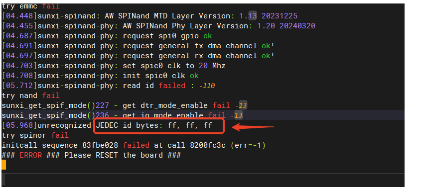
排查:读ID失败,且读出来是全FF,一般是硬件问题,检测 Flash 是否有虚焊,或者检查原理图接线是否正确,或者MUX是否正确。